Scanning Tunneling Microscopy
Researchers
Anjan Soumyanarayanan, Michael Yee, Yang He
Projects
- Topological insulators
- Charge density wave in NbSe2
- Fe-based superconductors
- Bi-based cuprate superconductors
- Instrument design
Topological Insulators
We are studying the spectroscopic properties of topological insulators (TIs) and topological metals (TMs) to understand the novel properties of the surface states, and to quantify the robustness of topological protection to chemical imperfections and magnetic fields.
As-doped Bi2Se3
Bi2Se3, a TI with a large band gap and simple band structure, is expected to be promising for technological applications. Our studies of As-doped Bi2Se3 below the Dirac point have revealed a strong, non-dispersive scattering mode at the onset of the bulk valence band. We find that the surface states are not robust to scattering into the bulk in the valence band regime. This has implications for the design of n-doped Bi2Se3 devices.
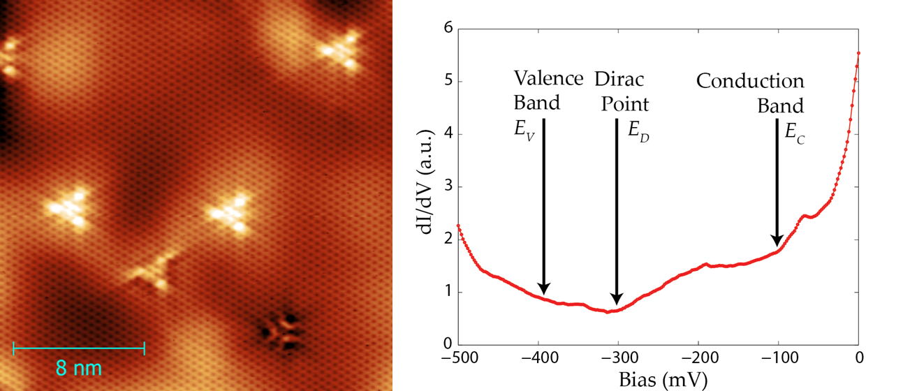
Fig. 1: Topography and spectroscopy Bi2Se3Asx (-100 mV, 1 GΩ, T=5K) (a) Atomically resolved STM topography showing a bright triangular impurities (identified as Se vacancies, and the dark clover-shaped impurities (identified as As dopants). (b) Point spectrum with identification of the bulk bands and the Dirac point.
Sb(111)
We are also studying the topological properties of the surface states in the semi-metal Sb(111). Due to the metallic nature of the bulk states, the surface states are only accessible to surface-sensitive techniques like STM.
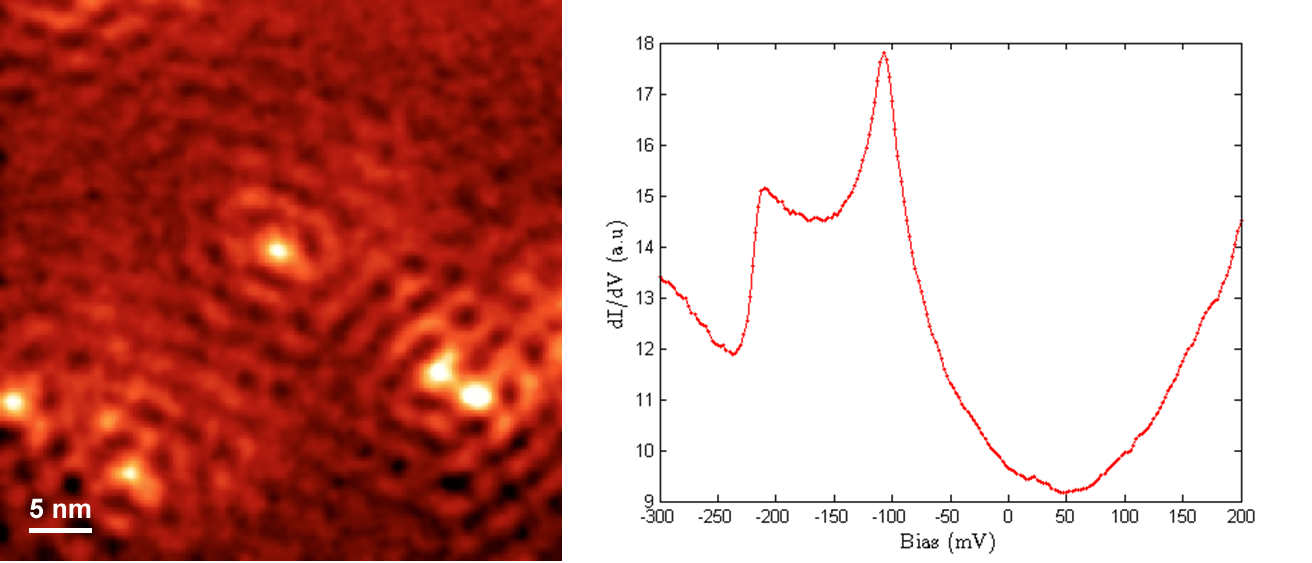
Fig. 2: Point spectrum and quasiparticle interference in Sb(111) (+250 mV, 0.25 GΩ, T=8K) (a) Conductance map (+75 mV) showing standing waves generated around impurities. (b) Point spectrum, with sharp kinks generated by the bulk valence band.
Collaborators
Young Lee, MIT
Yoichi Ando, Osaka University
Funding
NSF DMR-1106023
Charge Density Waves in NbSe2
NbSe2 is a conventional superconductor that also has a charge density wave (CDW) state, where every third atom appears brighter than the rest. The coexistence of this CDW state with a superconducting state could serve as a model system to help explain other superconductors that have proposed competing orders, such as cuprates and pnictides. To this end we have performed spectroscopic studies of NbSe2 around the CDW transition temperature (33K) from T=2K to 40K. Using scanning tunneling spectroscopy, we have mapped the local density of states vs. temperature and energy. Above the CDW transition temperature the CDW loses long-range coherence and is pinned to impurities. We have further studied the temperature dependence of the CDW spectral gap and have compared our results with tight-binding calculations.
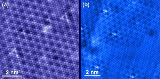
Fig. 3: Atomically resolved STM topographies (10 nm × 10 nm) of doped NbSe2, showing a hexagonal lattice and triangular impurities. (a) Topography taken at temperature below the CDW transition. The CDW is well defined and has a three-atom periodicity. (b) Topography taken at a temperature above the transition temperature. Above the transition the long-range phase coherence is broken and the CDW is pinned to impurities.
Collaborators
Kai Rossnagel & Dirk Rahn, Kiel University
Michael Norman & Jasper van Wezel, Argonne National Laboratory
Eric Hudson, Pennsylvania State University
Funding
NSF DMR-0847433
Vortex Imaging in Iron Pnictide Superconductor Ba(CoxFe1-x)2As2
The discovery of iron-arsenic based superconductors (pnictides) in early 2008 broke the monopoly that cuprates had held over high-temperature superconductivity for more than two decades and led to new hope that the study of pnictides as a foil for cuprates could lead to breakthroughs in the understanding of high temperature superconductors. Additionally, the pnictides are more isotropic in a magnetic field, which may facilitate application due to more effective pinning of quantized magnetic vortices whose motion causes dissipation.
We carried out a study of optimally doped BaFe1.8Co0.2As2 single crystals. The Co dopants reside in the more strongly bound Fe-As layer; therefore the cleaved surface retains the same doping as in the bulk. The Ba atoms remaining on the cleaved surface arrange into a stripelike 2×1 pattern. An atomic resolution topographic image is shown in Figs. 4a,b.
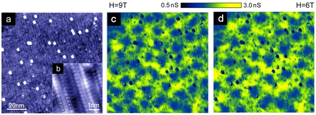
Fig. 4: STM images of BaFe1.8Co0.2As2. (a) 100 nm × 100 nm topography, showing single-atom impurities as bright white spots. (b) Magnified inset shows atomic resolution with 2×1 surface reconstruction. (c) and (d) dI/dV images at the coherence peak energy E=5meV, show vortices as broad blue regions of depressed conductance, at 9 Tesla and 6 Tesla, respectively.
We used spectroscopic imaging to study the magnetic vortices in this material. At 9T and 6T we imaged vortices electronically by mapping the conductance (proportional to the density of states) at an energy where a vortex destroys the coherence peak of the superconducting gap. Figs. 4c,d show differential conductance maps at E=5meV, where vortices are visible as dark features due to the local suppression of the density of states at this energy. The vortices form a disordered lattice, consistent with isotropic, single flux quantum vortices.
Much can be learned about vortex interactions and pinning by studying the locations of vortices with respect to each other and to other structures within the superconductor. Vortex interactions can be roughly categorized into three scenarios. In the absence of strong pinning sites, vortices crystallize into a hexagonal lattice, shown in schematically in Fig. 5a. In the presence of strong pinning sites, the vortex arrangement with respect to those sites depends on the anisotropy of the material. In highly anisotropic superconductors, a one-dimensional vortex line may split like a stack of pancakes into point-like objects with the freedom to move independently in each superconducting layer. In this scenario, pancakes may find pinning sites independently in each layer, resulting in a high correlation between observed vortex and pinning locations in any given layer. This scenario is shown schematically in Fig. 5b. Finally, in a more isotropic superconductor with strong pinning sites, the vortices must remain as line objects, and can bend only slightly between layers to maximize their overlap with impurities throughout the bulk. In this scenario, there may be very little observable correlation between vortex locations and impurities in any one layer. This third scenario is depicted schematically in Fig. 5c. As shown in our data in Figs. 4c,d the vortices in BaFe1.8Co0.2As2 form a disordered lattice, indicating strong pinning. There is no correlation between the locations of vortices and surface-impurities, proving that bulk pinning, and not surface pinning, must play a significant role in this superconductor. This third scenario is the most promising for technological applications because vortex motion causes dissipation and if vortices are pinned through several layers by a single pinning site it is far easier to engineer sufficient pinning sites.
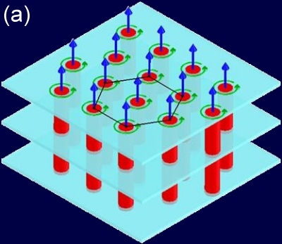
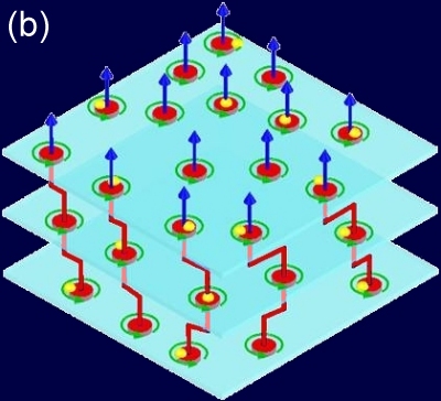
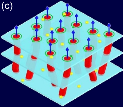
Fig. 5: Schematic illustrations of 3 different vortex pinning scenarios. (a) Negligible pinning; vortices form a lattice. (b) Strong pinning, large anisotropy; vortices separate into pancakes connected by Josephson vortices between layers. (c) Strong pinning, small anisotropy; vortices form a disordered lattice as they bend slightly to accommodate bulk pinning sites.
Past Researchers
Yi Yin, Martin Zech, Tess Williams
Collaborators
Xianhui Chen, University of Science & Technology, China
Funding
NSF DMR-0508812, AFOSR FA9550-05-1-0371
Vortex Liquid in Cuprate Superconductor Bi2Sr2CuO6+x
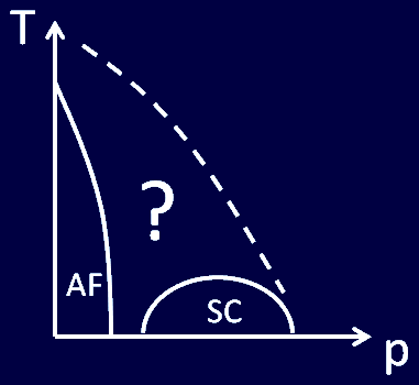
Fig. 6: Cuprate phase diagram: Temperature vs. doping.
The phase diagram of the cuprate superconductors contains, in addition to the antiferromagnetic and superconducting phases, a mysterious phase called the pseudogap (shown under the dashed line in the phase diagram in Fig. 4). In the pseudogap regime the density of states (DOS) is depressed at the Fermi level but transport measurements do not show bulk superconductivity. The apparent smooth evolution of the pseudogap down through the transition temperature into the superconducting gap has led some to argue that the pseudogap is a true pairing gap, a precursor to phase coherent superconductivity. Others have argued that the pseudogap is a signature of a competing or irrelevant phase. In either case, an understanding of the pseudogap will likely be a necessary precursor to a full theoretical description of cuprate superconductivity.
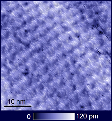
Fig. 7: Atomic resolution topography of the surface of (Bi1-yPby)2Sr2CuO6+x. (Pb doping is used to remove the supermodulation, but has no apparent effect on the density of state.)
Overdoped Bi2Sr2CuO6+x is a good material for studying the pseudogap phase. This cuprate is a layered material which cleaves on an atomically flat surface, exposing a clean and stable surface that is well-suited for STM studies, as shown in Fig. 5. The low superconducting Tc of 15K allows easy comparison of states inside and outside of the superconducting dome with minimal thermal broadening. The upper critical field Hc2 is also accessible, approximately 9 Tesla at liquid helium temperature.
In the Hudson lab's prior work [1] the temperature was tuned to compare the DOS in the superconducting dome to that directly above it in the pseudogap phase, symbolized by the red arrow in the three-dimensional phase diagram in Fig. 6. In a complementary study, we have used our STM to compare the DOS in the superconducting dome to the DOS at the same doping and temperature in magnetic fields up to 9T, essentially leaving the superconducting dome through a perpendicular path, as represented by the blue arrow. The critical factor in both of these studies is the ability to compare spectra at exactly the same spatial location as an external parameter is tuned. Cuprates exhibit an intrinsic nanoscale spatial inhomogeneity throughout the phase diagram. Maintaining spatial registry through changes in temperature or magnetic field is crucial in order to strip out the intrinsic inhomogeneity and clearly identify the changes that occur on crossing the superconducting Tc or Hc2.
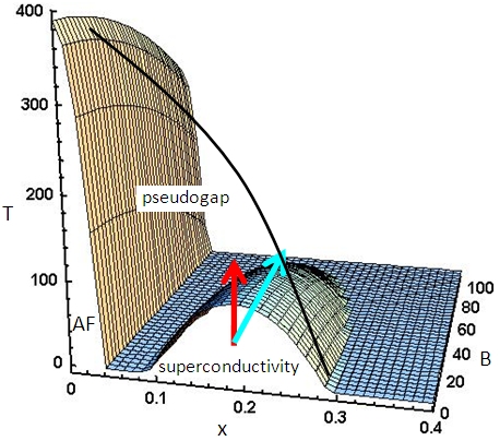
Fig. 8 3-dimensional phase diagram of cuprate superconductors, as a function of doping, temperature, and magnetic field.
At a temperature of 6 K, we find the gap depth from the spatially averaged dI/dV spectrum decreases with increasing magnetic field, which indicates a vortex liquid state. By tracking atomically resolved locations at different magnetic fields, we apply a normalization technique to remove inhomogeneities in the underlying density of states, revealing a more homogeneous superconducting state.
[1] M. C. Boyer, W. D. Wise, Kamalesh Chatterjee, Ming Yi, Takeshi Kondo, T. Takeuchi, H. Ikuta, E. W. Hudson, "Imaging the two gaps of the high-temperature superconductor Bi2Sr2CuO6+x". Nature Physics 3, 802 (2007). (link)
Past Researchers
Yi Yin, Martin Zech, Tess Williams
Collaborators
Hiroshi Ikuta, Nagoya University
Eric Hudson, Pennsylvania State University
Funding
NSF DMR-0508812, AFOSR FA9550-05-1-0371
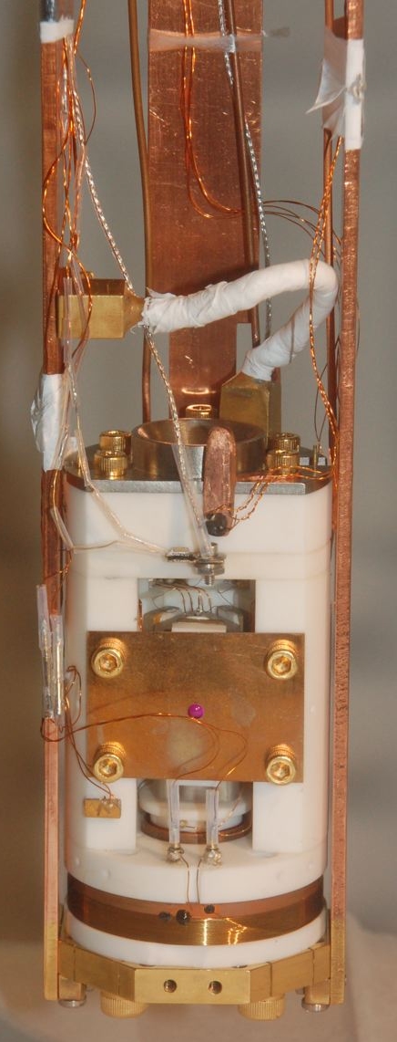
Fig. 9 Photograph of the STM built in the Hoffman lab.
Instrument
- Simple explanation of STM (no equations)
- Technical explanation of STM
- Measurements we can make with an STM
We have constructed a custom low temperature scanning tunneling microscope with the following features optimized for the study of cleavable correlated electron materials:
- Surface preparation: In-situ, low temperature sample cleaver for exposing a clean sample surface in a cryogenic ultra-high vacuum (UHV) environment.
- Vibration isolation: floating room, floating table.
- Temperature: At present we have tested temperatures from 1.2K up to 50K. We are in the process of implementing a 3He system, which will run down to 500 mK in continuous operation. Our STM can track the same atomically resolved locations throughout the temperature range.
- Magnetic field: 9 Tesla vertical, and 3 Tesla rotatable in-plane. Our STM can track the same atomically resolved locations as the field is swept over the full range.
Funding
The researchers acknowledge support from Merck, the Harvard University Center for the Environment (HUCE), the Agency for Science Technology and Research (A*STAR), and the Natural Sciences and Engineering Research Council of Canada (NSERC).