Force Microscopy
Researchers
Sarah Schlotter, Harry Mickalide, Magdalena Huefner
Projects
Insulator-Metal Transition in VO2
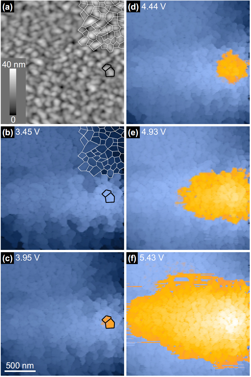
Fig. 3(a) AFM topography of the VO2 surface. [(b)-(f)] Current maps at increasing bias voltage show the metallic puddle seeded at two grains (outlined in black), growing with increasing bias. Blue and yellow regions correspond respectively to low and high current.
Vanadium dioxide (VO2) is a strongly correlated transition metal oxide that undergoes a structural and electronic phase transition near T = 340 K. In this insulator-to-metal transition (IMT), the resistivity of VO2 decreases by up to 5 orders of magnitude. Understanding the details of this transition has both scientific and practical importance, due to the variety of potential technological applications of this material.
The goal of our research on this material is to understand the physics of the IMT by studying the local electronic properties of VO2 thin films. To acquire spatially resolved information about the electronic transition, we use an atomic force microscope (AFM) with a conducting cantilever in contact mode. First, we apply a constant bias voltage between tip and sample, and map the resultant current at each location on the sample. The series of maps shown in Figure 3 illustrates the growth of the metallic region of the sample as we increase the applied voltage. In a second operating mode, we trigger the IMT by varying the bias while at a fixed location. The I-V curves shown in Figure 4 demonstrate our ability to simultaneously alter and measure the local conducting state of the VO2 sample. A full map of such I-V curves enables us to pull out images of a number of different electronic properties. For example, Fig. 5 shows the locally applied voltage at which the sample undergoes the IMT. Using maps such as these, we are working to correlate local properties to better understand the physics of the IMT and associated structural transition in VO2.
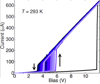
Fig. 4 200 consecutive IV sweeps at room temperature at a single location on the VO2 sample, in conducting-AFM geometry.
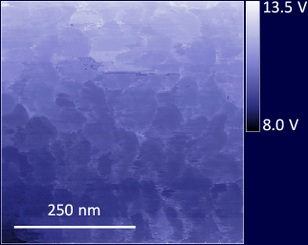
Fig. 5 Map of insulator-to-metal transition voltages determined from I-V curves measured at each location on the sample.
Past researchers
Jeehoon Kim (now at Los Alamos National Lab)
Alex Frenzel (now at MIT)
Collaborators
Shriram Ramanathan (Harvard University)
Changhyun Ko (Harvard University)
You Zhou (Harvard University)
Magnetic Materials Research: Nd2Fe14B
We are currently investigating the fractal domain structure of single-crystal Nd2Fe14B using magnetic force microscopy (MFM). Previous studies have demonstrated that thermally demagnetized samples of Nd2Fe14B have a high degree of fine-scale (~25nm) magnetic texture at surfaces perpendicular to the easy axis. The domains are organized in beautiful fractal-like patterns, with wavy rick-rack features at small length scales (see e.g. Kreyssig et al. PRL 102, 047204 (2009).). Fig. 6 shows a representative image of the fractal domain pattern, obtained with magneto-optic Kerr effect microscopy. Fig. 7 shows our MFM image of similar features zoomed in at ~40 times magnification. Our experiment uses cantilever tips with higher magnetic coercivity than previous studies. We hope to manipulate domain walls and understand their influence on the fractal domain pattern.

Fig. 6 Magneto-optic Kerr effect image of the fractal domain pattern of Nd2Fe14B taken in the group of our collaborator Prof. Ruslan Prozorov. The black box shows the approximate size (not the location) of the scan frame shown in Fig. 7.
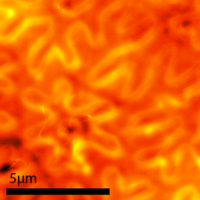
Fig. 7 Image of the wavy domain pattern of Nd2Fe14B taken with our magnetic force microscope.
Collaborators
Ruslan Prozorov (Ames Lab, Iowa State University)
Paul Canfield (Ames Lab, Iowa State University)
Instrument Design
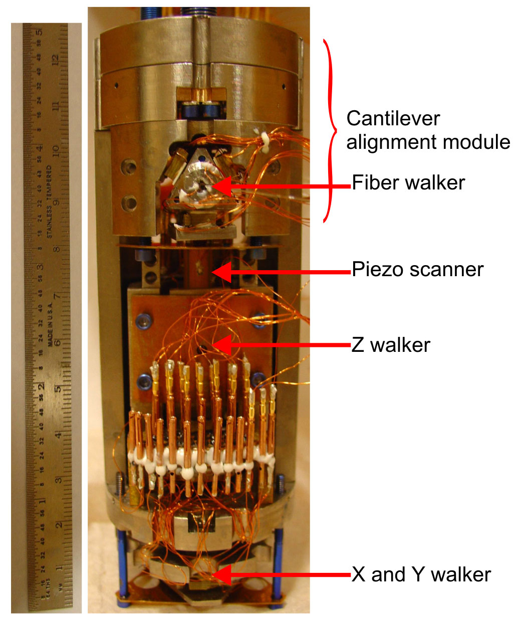
Fig. 8 Photo of force microscope.
We have constructed a custom variable temperature force microscope with the following features:
- Vibration isolation: floating room, floating table, internal suspension from damped springs.
- Temperature: 2K to above 340K
- Magnetic field: 5 Tesla vertical
- Scan Range: 35μm scan at room temperature;
several mm coarse (x ,y ,z ) motion of sample with respect to tip - Cantilever position detection:
fiber optic interferometer with λ=1550nm diode laser;
position noise better than 2×10⁻³ Å/√Hz - Geometry: allows either horizontal or vertical cantilever orientation
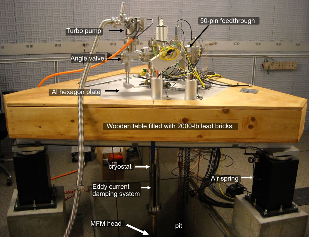
Fig. 9 Photo of force microscope setup, including vibration isolation.
Funding
Harvard NSEC, Sloan Foundation Fellowship, DFG (German Research Foundation) Fellowship, Merck Fund