Force Microscopy
Researchers
Maoz Ovadia, Jessie Zhang
Instrument Design
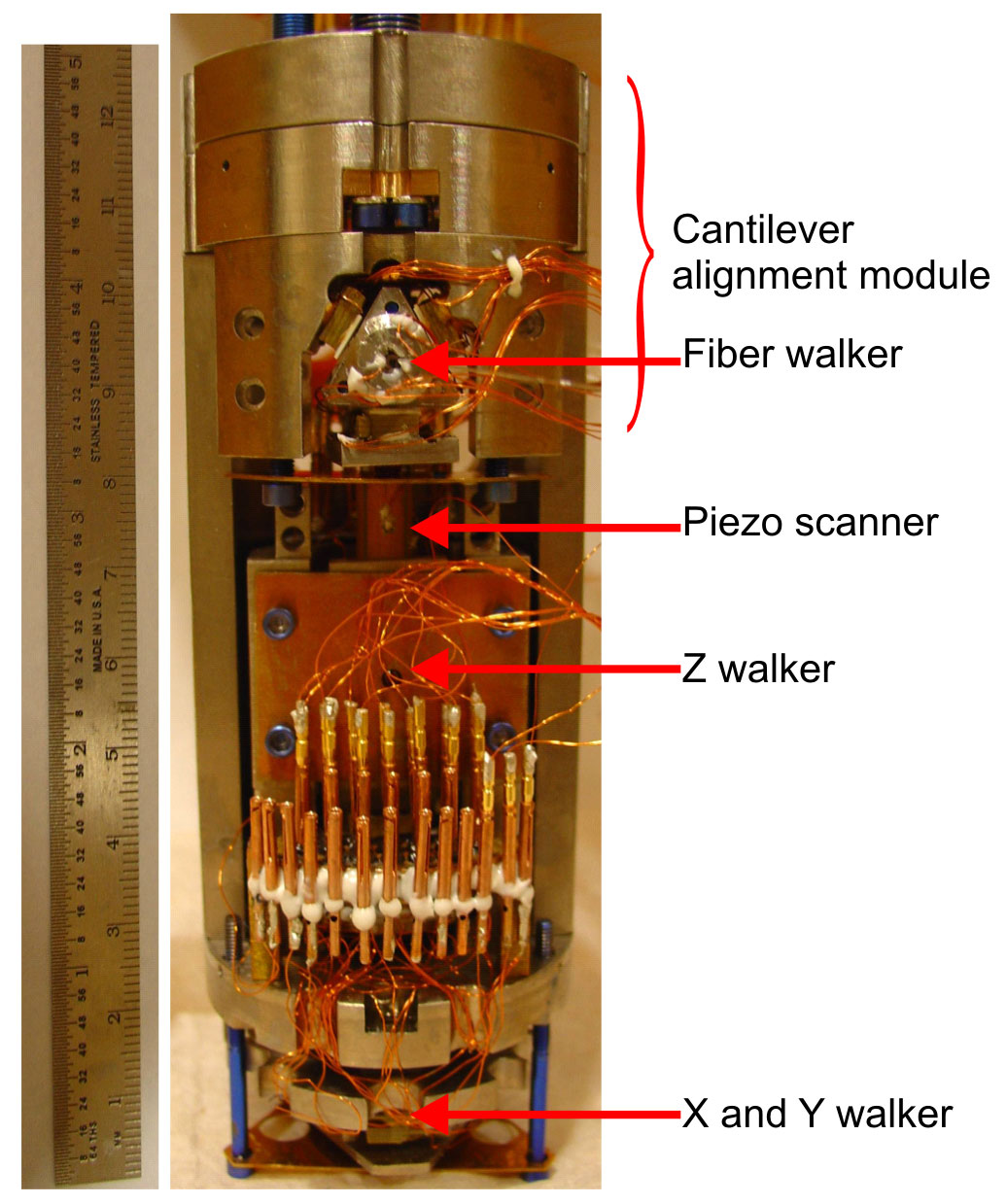
Fig. 1 Photo of force microscope.
We have constructed a custom variable temperature force microscope with the following features:
- Vibration isolation: floating room, floating table, internal suspension from damped springs.
- Temperature: 2K to above 340K
- Magnetic field: 5 Tesla vertical
- Scan Range: 35μm scan at room temperature;
several mm coarse (x ,y ,z ) motion of sample with respect to tip - Cantilever position detection:
fiber optic interferometer with λ=1550nm diode laser;
position noise better than 2×10⁻³ Å/√Hz - Geometry: allows either horizontal or vertical cantilever orientation
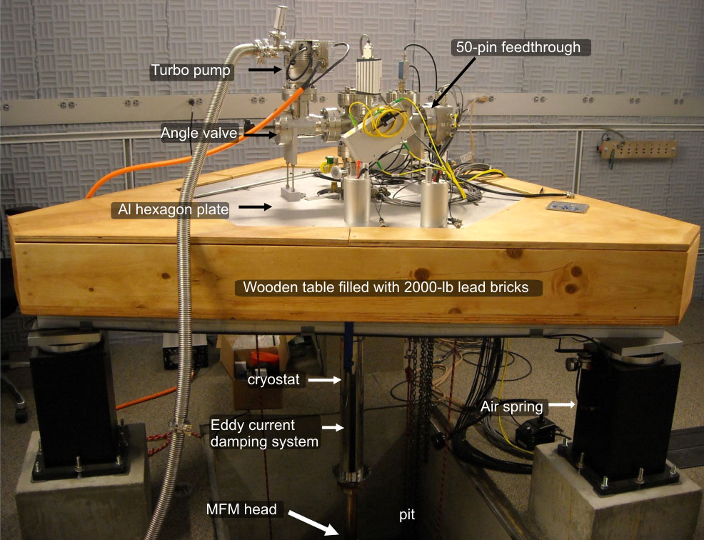
Fig. 2 Photo of force microscope setup, including vibration isolation.